PCB Designer Cover Letter Example

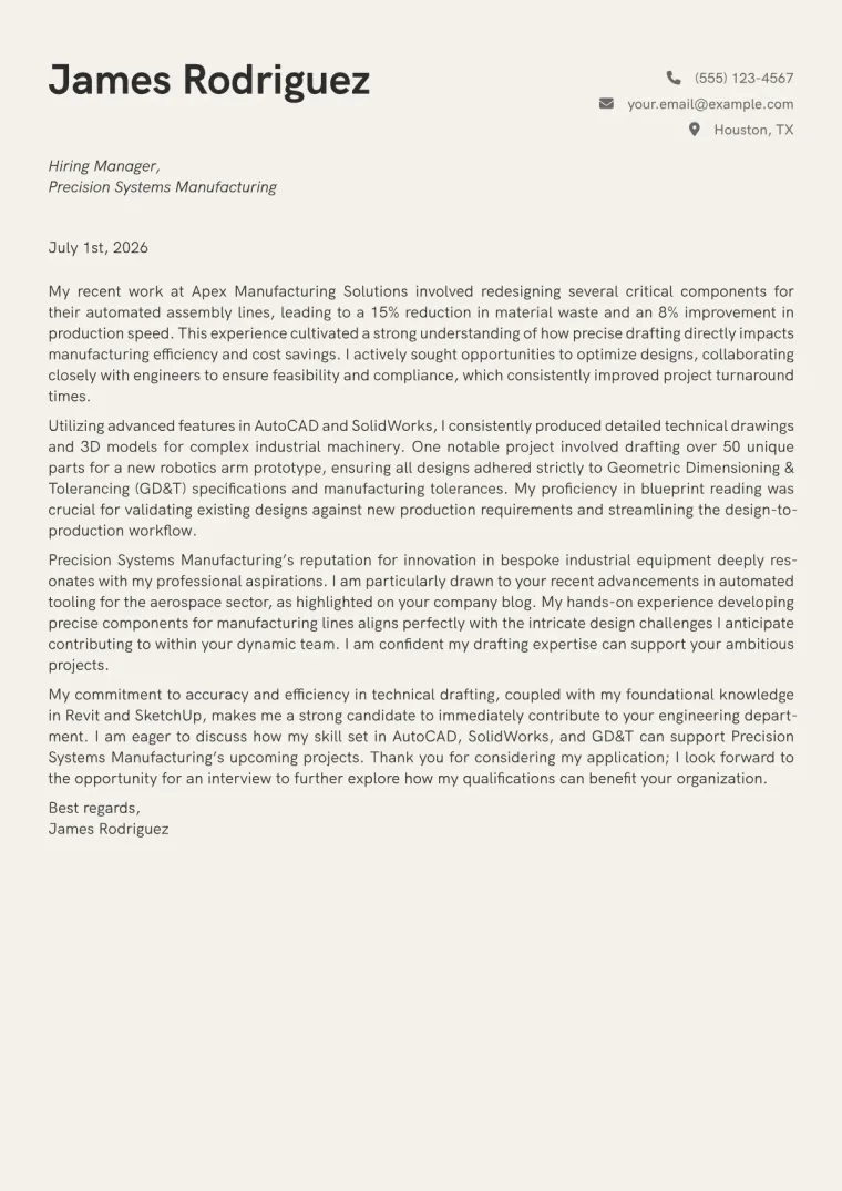
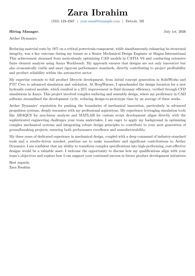
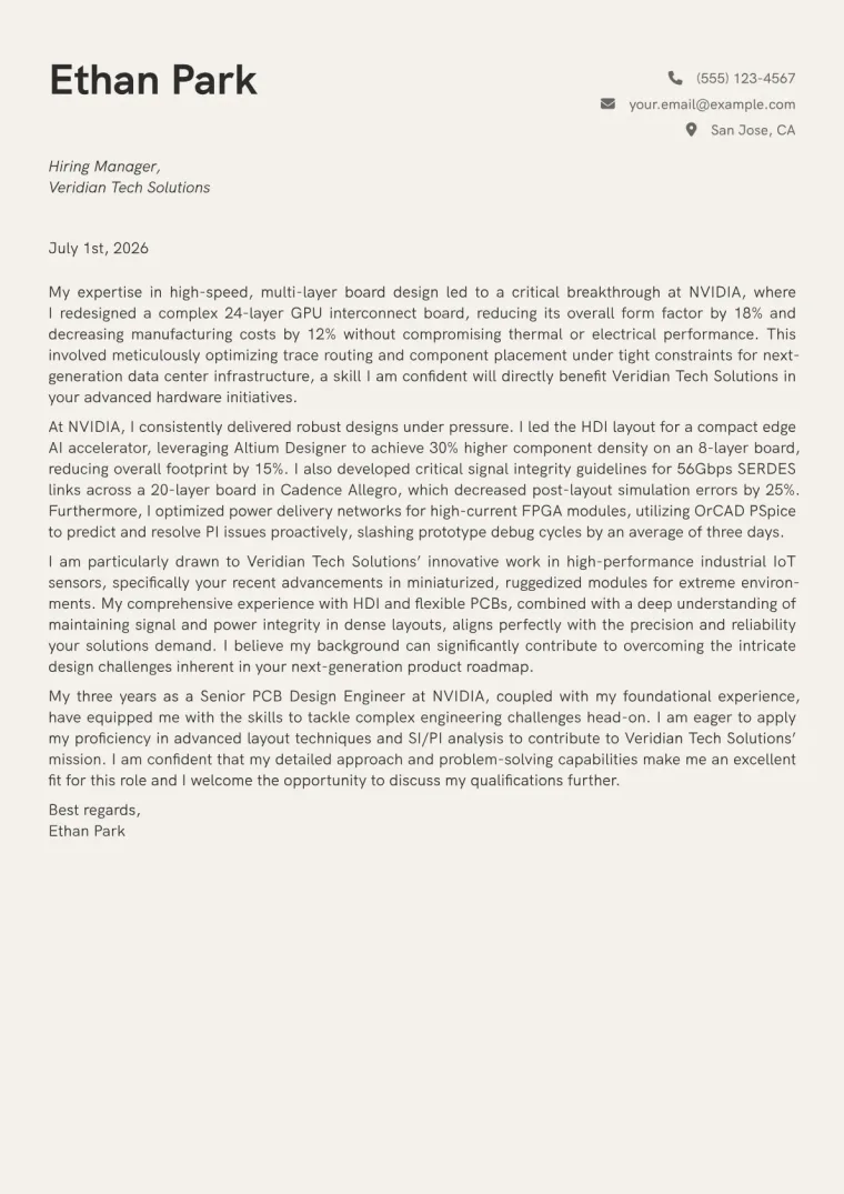
Three complete letters, each written for a different situation, in a different design.

PCB Designer cover letter example

Elena VolkovTo the Hiring Manager, Infinium Electronics

Achieving a 15% improvement in signal integrity across high-speed interfaces while concurrently optimizing board layers from 12 to 10 has been a consistent focus in my PCB design career. As a PCB Design Engineer at NVIDIA, I specialize in crafting complex, multi-layer layouts that not only meet stringent performance requirements but also enhance manufacturability and cost efficiency. My systematic approach to design challenges ensures robust solutions for cutting-edge technology, particularly in high-density computing environments where reliability is paramount.

My recent work included leading the PCB layout for a critical AI accelerator, where I meticulously managed power distribution networks and impedance control for 16 high-speed DDR5 channels. Leveraging Altium Designer, I reduced the board footprint by 10% and manufacturing cycle time by 7% through strategic component placement and advanced routing techniques, all while meeting strict thermal dissipation targets. This project demanded expert application of signal integrity analysis and careful mitigation of electromagnetic interference (EMI) in a compact form factor.

Infinium Electronics’ commitment to innovation in compact, high-performance embedded systems, exemplified by your groundbreaking work on the Aegis sensor platforms, perfectly aligns with my expertise in miniaturized, high-reliability designs. My extensive experience with OrCAD Allegro and PADS Layout, specifically in managing complex designs with tight space constraints and stringent environmental specifications, would directly benefit your team. I am particularly drawn to your focus on integrating advanced RF components, an area where my signal integrity and power integrity skills are highly relevant.

My proficiency in Altium Designer, OrCAD Allegro, and advanced SI/PI analysis, combined with a track record of delivering optimized, production-ready designs, positions me to make immediate contributions to Infinium Electronics. I am eager to apply my skills in tackling the intricate design challenges your firm addresses. I look forward to discussing how my five years of experience can support your mission and contribute to your next generation of innovative products.

Best regards,
Elena Volkov
PCB Designer cover letter for a career changer

Elena VolkovTo the Hiring Manager, NexaCore Systems

I bridge the gap between structural integrity and electronic functionality, a technical discipline that recently allowed me to optimize enclosure airflow for high-density hardware, cutting thermal failure rates by 22 percent during prototyping. This hands-on experience with product development cycles informs my entry into the PCB Designer role at NexaCore Systems. By applying the rigor of mechanical tolerances to schematic capture and layout, I translate electrical requirements into board designs that minimize manufacturing defects. My commitment to technical precision ensures that every component is placed with exact consideration for physical and electrical constraints.

During my certification training and intensive personal projects, I successfully migrated a complex legacy board design from Eagle CAD to Altium Designer, achieving a 100 percent connectivity accuracy rate across four high-speed differential pairs. I utilized OrCAD Allegro to implement a controlled impedance stack-up that satisfied strict EMI requirements for a wireless sensor module. Furthermore, I validated power integrity using simulation tools to resolve a voltage droop issue on an FPGA board. These technical tasks demonstrate my proficiency in translating logical designs into reliable hardware while maintaining strict signal integrity throughout the layout process.

NexaCore Systems leads the industry in modular industrial automation, which requires the exact type of dense, heat-sensitive circuitry I am eager to refine. My mechanical engineering background grants me a unique advantage in understanding board-to-enclosure thermal dissipation and physical vibration resistance that most designers overlook. Combining this insight with my newly refined capabilities in PADS Layout, I am ready to support your development of high-reliability controllers. I view the challenge of shrinking board footprints while maintaining structural and signal robustness as the natural evolution of my career path toward high-performance electronics design.

My decision to focus on board-level design is rooted in a desire to maximize the efficiency of hardware performance at the source. I bring a deliberate, analytical mindset to every layout iteration, ensuring that your team maintains its competitive edge through error-free design execution. I look forward to discussing how my combination of mechanical intuition and electronic design skill will contribute to your upcoming projects at NexaCore Systems. Please reach out to schedule a time when I can demonstrate the portfolio of designs I have constructed during my formal certification and independent projects.

Best regards,
Elena Volkov

PCB Designer cover letter with no experience

Elena VolkovTo the Hiring Manager, NexTech Silicon

My senior capstone project necessitated a 22 percent reduction in crosstalk on a four layer board to ensure reliable signal integrity for a high speed data acquisition system. Achieving this target required meticulous trace impedance control and several iterations of layout simulation. By refining these signal paths, I successfully transformed an unstable prototype into a robust platform for robotics research. This experience fostered a deep understanding of board level hardware complexities and directly informs my approach to maintaining signal integrity within tight manufacturing constraints while adhering to strict industry standards.

My recent technical project work reflects a commitment to precision and efficient routing. During a personal robotics challenge, I optimized a sensor controller board by shrinking its surface area by 30 percent while maintaining full EMI/EMC compliance. Utilizing Altium Designer, I successfully routed 150 components with 0402 footprints, ensuring minimal thermal hotspots. Furthermore, I migrated a legacy schematic from KiCad to OrCAD Allegro to resolve routing constraints that improved trace connectivity by 15 percent. These tasks demonstrate my proficiency in navigating complex design constraints through a disciplined focus on logical layout and signal integrity analysis.

NexTech Silicon stands out as an innovator in the field of compact sensor integration because your team prioritizes modularity while minimizing footprint. Your recent work on the modular sensor array for edge computing requires exactly the type of precise, dense routing that I have spent the last year perfecting. My technical mastery of PADS Layout and my background in electromagnetic compatibility testing are uniquely aligned with your current production goals. I am eager to contribute my technical rigor to a team that consistently pushes the boundaries of hardware design efficiency and reliability.

The opportunity to demonstrate my capability for your design team aligns with my professional goals as an emerging engineer in the Silicon Valley ecosystem. I am prepared to apply my technical foundation to support the development of your next generation hardware projects immediately. My resume provides additional context regarding my completed coursework and technical certifications. I look forward to discussing how my specific design experiences can contribute to your upcoming product releases. Please let me know when you are available for an interview to review my design portfolio in greater detail.

Best regards,
Elena Volkov

Editorial Notes

For a PCB Designer role, hiring managers in the Technology industry seek concrete evidence of a candidate's technical prowess and direct impact on product development. They prioritize quantified achievements in areas such as signal integrity, board layer optimization, and efficient management of high-speed interfaces. Expertise with industry-standard tools like Altium Designer, OrCAD Allegro, or PADS Layout is crucial, alongside a demonstrated ability to tackle complex challenges like power distribution networks, impedance control, EMI mitigation, and thermal dissipation. Achievements that directly translate to enhanced manufacturability, reduced board footprint, or shortened manufacturing cycle times are highly valued signals of an effective designer.

This example letter excels by immediately grabbing attention with a quantified opening hook detailing a 15% signal integrity improvement and board layer optimization. The subsequent paragraph provides robust evidence mirroring core PCB design duties, illustrating leadership on an AI accelerator project, meticulous DDR5 channel management, and a 10% board footprint reduction achieved with Altium Designer. It then articulates a specific, well-researched rationale for applying to Infinium Electronics, aligning personal expertise with the company's work on Aegis sensor platforms. The letter concludes with a confident assertion of immediate value and eager anticipation for further discussion.

This meticulously crafted letter pairs seamlessly with JobSprout's PCB Designer resume example. Users can adapt this framework and incorporate their own accomplishments using JobSprout's AI cover letter writer to generate personalized applications.

Frequently Asked Questions

What is the best way to open a PCB Designer cover letter?
Start with a strong, quantifiable achievement or a specific skill relevant to the job, immediately demonstrating your value without using generic phrases like 'I am writing to express my interest.' Focus on an outcome you achieved.
How can I make my experience sound specific and not just a list of tools?
Instead of just listing tools, describe how you used them on a specific project. For example, 'Leveraging Altium Designer, I reduced the board footprint by 10%...' instead of just 'Proficient in Altium Designer.' Quantify the impact and outcome of your work.
Should I mention all my PCB design tools in the letter?
Prioritize the tools most relevant to the job description and those you have used to achieve significant results. Grouping them or mentioning them in the context of projects works better than a simple list. Elena mentioned Altium, OrCAD, and PADS, which are key for her level.
How do I tailor the cover letter to a specific company as a PCB Designer?
Research the company's specific products, projects, or technological focus. Then, connect your skills and experience directly to those areas. Mentioning their 'Aegis sensor platforms' shows you've done your homework and understand their work.
What kind of 'quantified achievements' are relevant for a mid-level PCB Designer?
Focus on metrics like percentage reduction in board size or layers, improvement in signal integrity, cost savings, or reduction in manufacturing cycle time. These demonstrate tangible contributions and problem-solving abilities.

More Technology cover letter examples