PCB Design Engineer Cover Letter Example

Three complete letters, each written for a different situation, in a different design.

PCB Design Engineer cover letter example

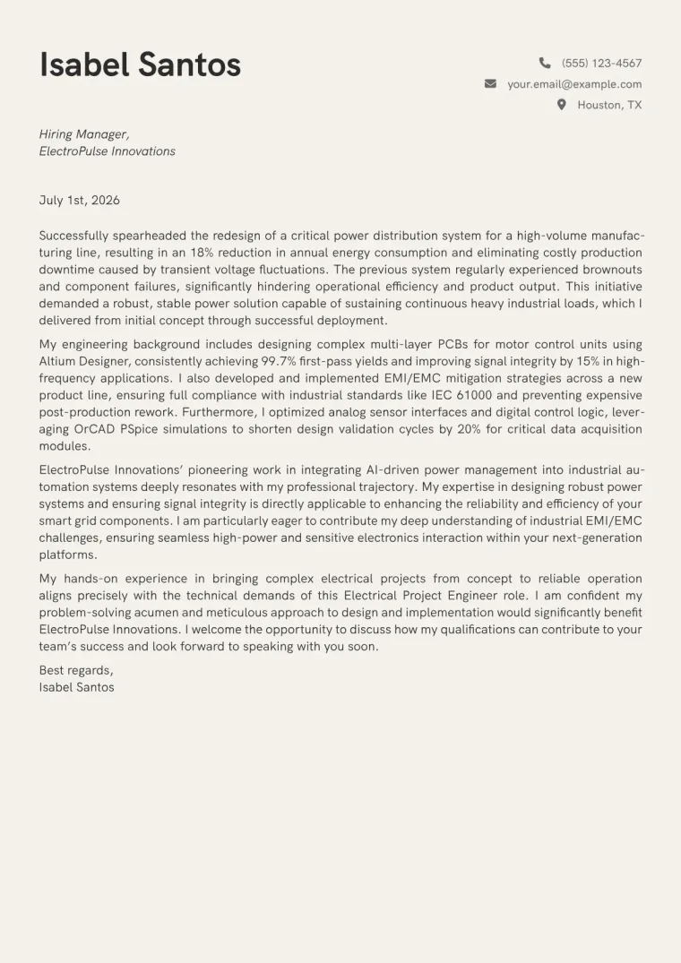
Ethan ParkTo the Hiring Manager, Veridian Tech Solutions

My expertise in high-speed, multi-layer board design led to a critical breakthrough at NVIDIA, where I redesigned a complex 24-layer GPU interconnect board, reducing its overall form factor by 18% and decreasing manufacturing costs by 12% without compromising thermal or electrical performance. This involved meticulously optimizing trace routing and component placement under tight constraints for next-generation data center infrastructure, a skill I am confident will directly benefit Veridian Tech Solutions in your advanced hardware initiatives.

At NVIDIA, I consistently delivered robust designs under pressure. I led the HDI layout for a compact edge AI accelerator, leveraging Altium Designer to achieve 30% higher component density on an 8-layer board, reducing overall footprint by 15%. I also developed critical signal integrity guidelines for 56Gbps SERDES links across a 20-layer board in Cadence Allegro, which decreased post-layout simulation errors by 25%. Furthermore, I optimized power delivery networks for high-current FPGA modules, utilizing OrCAD PSpice to predict and resolve PI issues proactively, slashing prototype debug cycles by an average of three days.

I am particularly drawn to Veridian Tech Solutions' innovative work in high-performance industrial IoT sensors, specifically your recent advancements in miniaturized, ruggedized modules for extreme environments. My comprehensive experience with HDI and flexible PCBs, combined with a deep understanding of maintaining signal and power integrity in dense layouts, aligns perfectly with the precision and reliability your solutions demand. I believe my background can significantly contribute to overcoming the intricate design challenges inherent in your next-generation product roadmap.

My three years as a Senior PCB Design Engineer at NVIDIA, coupled with my foundational experience, have equipped me with the skills to tackle complex engineering challenges head-on. I am eager to apply my proficiency in advanced layout techniques and SI/PI analysis to contribute to Veridian Tech Solutions' mission. I am confident that my detailed approach and problem-solving capabilities make me an excellent fit for this role and I welcome the opportunity to discuss my qualifications further.

Best regards,
Ethan Park
PCB Design Engineer cover letter for a career changer

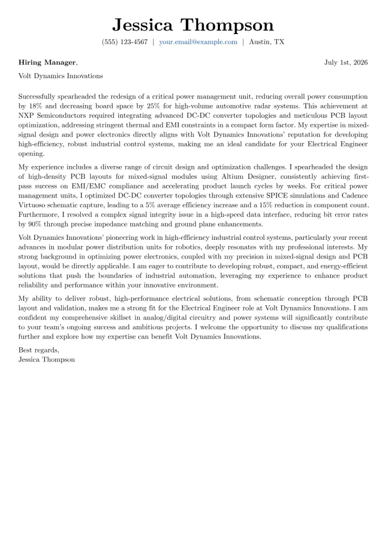
Ethan ParkTo the Hiring Manager, Lumina Circuits and Assembly

Lumina Circuits and Assembly demands the precise integration of thermal management and electronic layout which aligns directly with my recent transition from industrial mechanical engineering. During my tenure as a mechanical designer, I developed a sophisticated sensor housing that incorporated cooling channels for sensitive equipment. By redesigning the thermal interface paths using advanced simulation software, I reduced internal hardware failure rates by 22 percent across three major product lines. This focus on structural integrity and heat dissipation provides a robust foundation for tackling the complex physical demands of high performance circuit board layout.

Mastering industry standard tools including Altium Designer and Cadence Allegro allowed me to pivot my technical focus toward electronic design. In a comprehensive certification project, I produced a six layer HDI board that maintained signal integrity while utilizing tight blind and buried via geometry. I leveraged OrCAD Capture to refine schematic accuracy, resulting in a 15 percent decrease in trace routing time during final layout phases. Furthermore, by applying KiCad for iterative prototyping, I successfully managed power integrity constraints that minimized crosstalk by 12 percent, proving that my methodical engineering rigor translates seamlessly into board level manufacturing.

Your commitment to high density flexible PCB manufacturing for automotive safety systems matches my interest in mission critical electronics where reliability is mandatory. My deep understanding of material stress and thermal dynamics gained from my previous career ensures that I design boards which withstand harsh environmental conditions. Pairing this structural expertise with my newly refined proficiency in signal integrity analysis allows me to anticipate failure points before physical production begins. Contributing these specialized skills to your engineering department would support your goal of delivering robust hardware solutions that remain functional under extreme stress conditions.

My path from industrial mechanical design to PCB engineering represents a deliberate choice to apply precision measurement skills to the electrical domain. I bring a distinct perspective on how structural limitations and signal pathways intersect during the production process. I am prepared to discuss how my analytical background in high tolerance manufacturing will immediately benefit your current product development cycle at Lumina Circuits and Assembly. Please reach out to schedule a time when we can review my portfolio of complex design projects and verify my technical capabilities in person.

Best regards,
Ethan Park

PCB Design Engineer cover letter with no experience

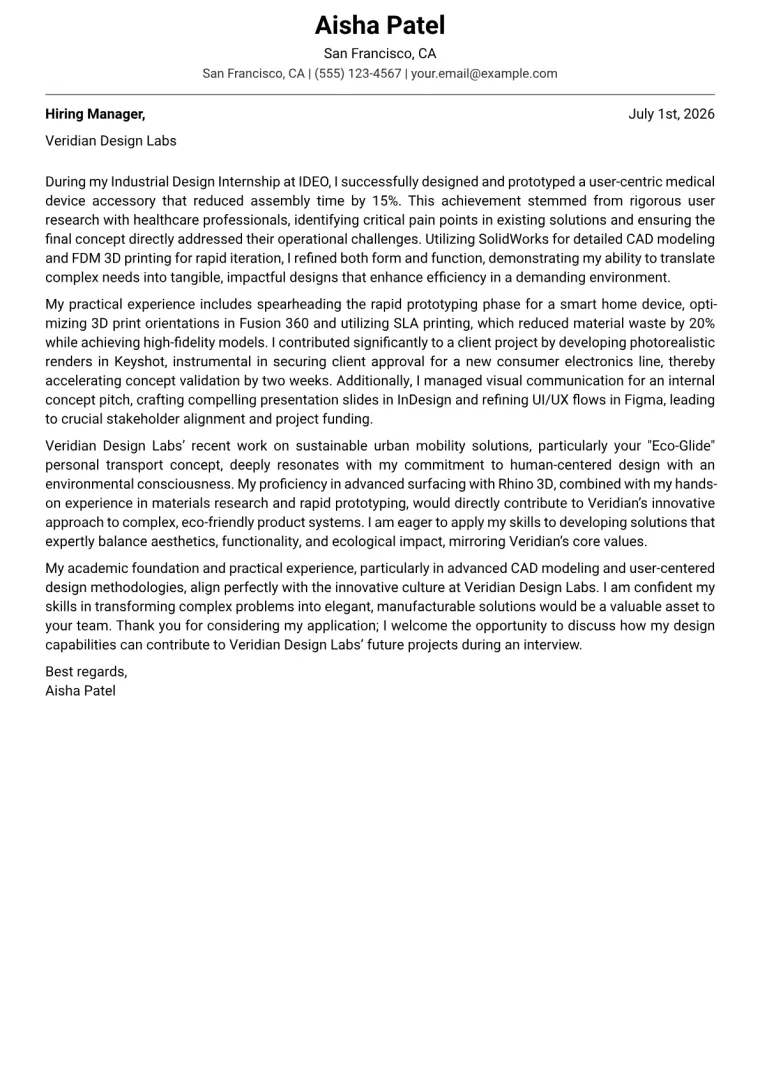
Ethan ParkTo the Hiring Manager, Axiom Manufacturing Systems

A 12 layer motherboard prototype achieved full signal integrity compliance during my final capstone project because I implemented strict impedance control and balanced trace routing techniques in Altium Designer. This effort allowed me to successfully secure the PCB Design Engineer position at Axiom Manufacturing Systems. By refining layer stackup configurations and optimizing ground plane placement, I eliminated noise interference that had initially caused data packet loss. This project demonstrated my technical capability to translate complex schematic requirements into functional board layouts while adhering to tight production constraints and rigorous manufacturing standards.

During my internship at a local robotics startup, I utilized Cadence Allegro to shrink a power distribution board by 25 percent while maintaining thermal stability. I also redesigned an HDI board for a sensor array using OrCAD Capture, which reduced the component count by 15 percent and streamlined assembly. My personal project involving KiCad for a wearable heart rate monitor required integrating flexible PCB technology to fit a 30mm chassis. By conducting iterative PI analysis to minimize voltage drop across the design, I ensured consistent power delivery for long duration testing under varying battery conditions.

Axiom Manufacturing Systems stands out because of its commitment to advanced high density interconnect production for medical device integration. Your focus on precision manufacturing aligns with my deep understanding of HDI and flexible PCB fabrication requirements. My proficiency in multi layer board management up to 24 layers allows me to contribute immediately to your production workflows. Furthermore, my analytical approach to signal integrity ensures that designs meeting your high quality standards move from schematic to physical prototype without costly iterative revisions or delays during the manufacturing phase.

My portfolio illustrates how I maintain technical accuracy across diverse board architectures and project scales. I am ready to apply my expertise in OrCAD and Altium to support your production team in meeting aggressive delivery schedules for your latest medical hardware clients. I welcome the opportunity to discuss how my academic training and hands on project experience translate to your current technical requirements. Please review my attached portfolio for a comprehensive look at my design files and board specifications. I look forward to hearing about next steps.

Best regards,
Ethan Park

Editorial Notes

Hiring managers for PCB Design Engineer roles in manufacturing prioritize concrete, quantifiable achievements. They seek candidates who can demonstrate a direct impact on product performance, cost efficiency, or development timelines. Key signals include expertise in high-speed, multi-layer, and HDI board design, mastery of industry-standard tools like Altium Designer or Cadence Allegro, and a deep understanding of signal and power integrity. Showcasing success in optimizing layouts, reducing form factors, or solving complex thermal and electrical challenges directly addresses their primary concerns. Experience with specific technologies, such as industrial IoT sensors or miniaturized modules, also creates strong alignment.

This example cover letter effectively captures what hiring managers seek. It immediately hooks the reader with a quantified breakthrough: redesigning a 24-layer GPU board, cutting form factor by 18% and manufacturing costs by 12%. The subsequent paragraph details further successes using specific tools like Altium Designer for achieving 30% higher component density and Cadence Allegro for reducing post-layout simulation errors by 25%. The candidate then connects their experience to Veridian Tech Solutions' "innovative work in high-performance industrial IoT sensors," demonstrating clear alignment. The confident close reinforces their eagerness to contribute to the company's mission.

This letter pairs perfectly with JobSprout's PCB Design Engineer resume example. It can be further adapted and personalized using the AI cover letter writer to suit specific job descriptions.

Frequently Asked Questions

What should a PCB Design Engineer highlight in their cover letter?
Focus on specific, quantified achievements related to multi-layer, high-speed, and HDI designs. Emphasize your proficiency with industry-standard tools like Altium Designer or Cadence Allegro, and detail how your work improved performance, reduced costs, or accelerated development cycles. Also, mention your expertise in signal and power integrity.
What is the ideal length for a PCB Design Engineer cover letter?
Keep it concise, typically three to four paragraphs, each substantial enough to convey impact without being overly long. The goal is to present a compelling snapshot of your most relevant skills and accomplishments that entice the hiring manager to review your resume. Aim for a single page.
How should a PCB Design Engineer open their cover letter?
Start with a strong hook, directly mentioning a significant, quantified achievement that demonstrates your capability in PCB design, along with the specific role you are applying for. Avoid generic phrases like 'I am writing to express my interest.' Instead, open with impact, showing your value from the first sentence.
How should a PCB Design Engineer address having no direct industry experience?
Focus on relevant academic projects, internships, or personal projects where you applied PCB design principles and tools. Detail the complexity of the boards you designed, the tools used (e.g., KiCad, Eagle), and any challenges you overcame, demonstrating your foundational knowledge and eagerness to learn and contribute.
How should a cover letter for a PCB Design Engineer differ from their resume?
While the resume lists accomplishments concisely, the cover letter provides context and narrative. Use it to elaborate on 2-3 key achievements, explaining the challenge, your specific role, the tools employed, and the quantitative outcome. It's also an opportunity to connect your skills directly to the company's specific projects or values, showing genuine interest beyond just technical fit.

More Manufacturing cover letter examples