PCB Design Engineer Resume Example
 Example by JobSprout
Market Insights
PCB Design Engineer
Salary Range
US market data · Source: Adzuna · Updated Mar 2026
How useful was this template?
PCB Design Engineer resume samples
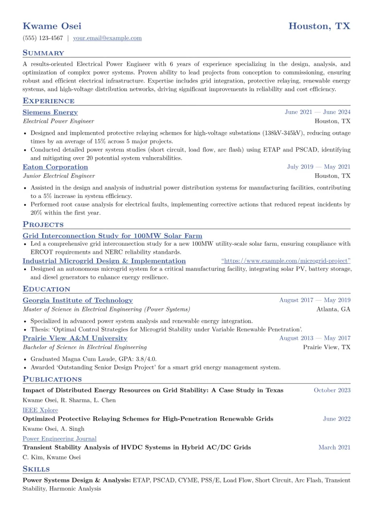
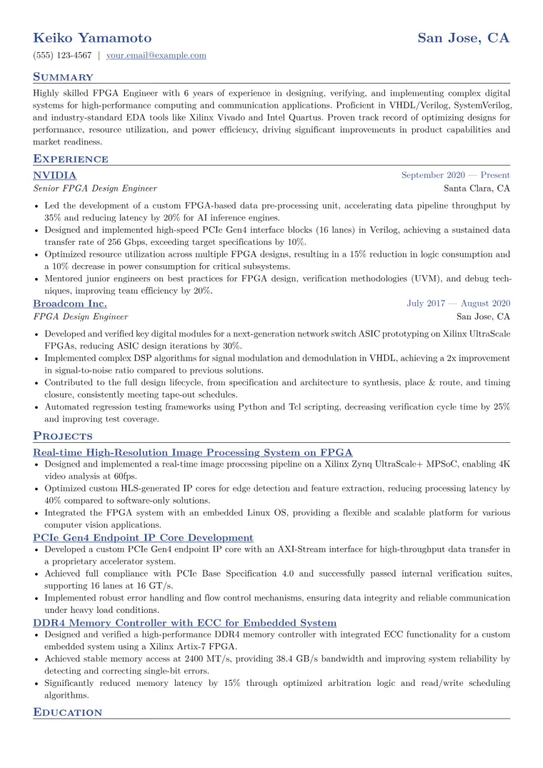
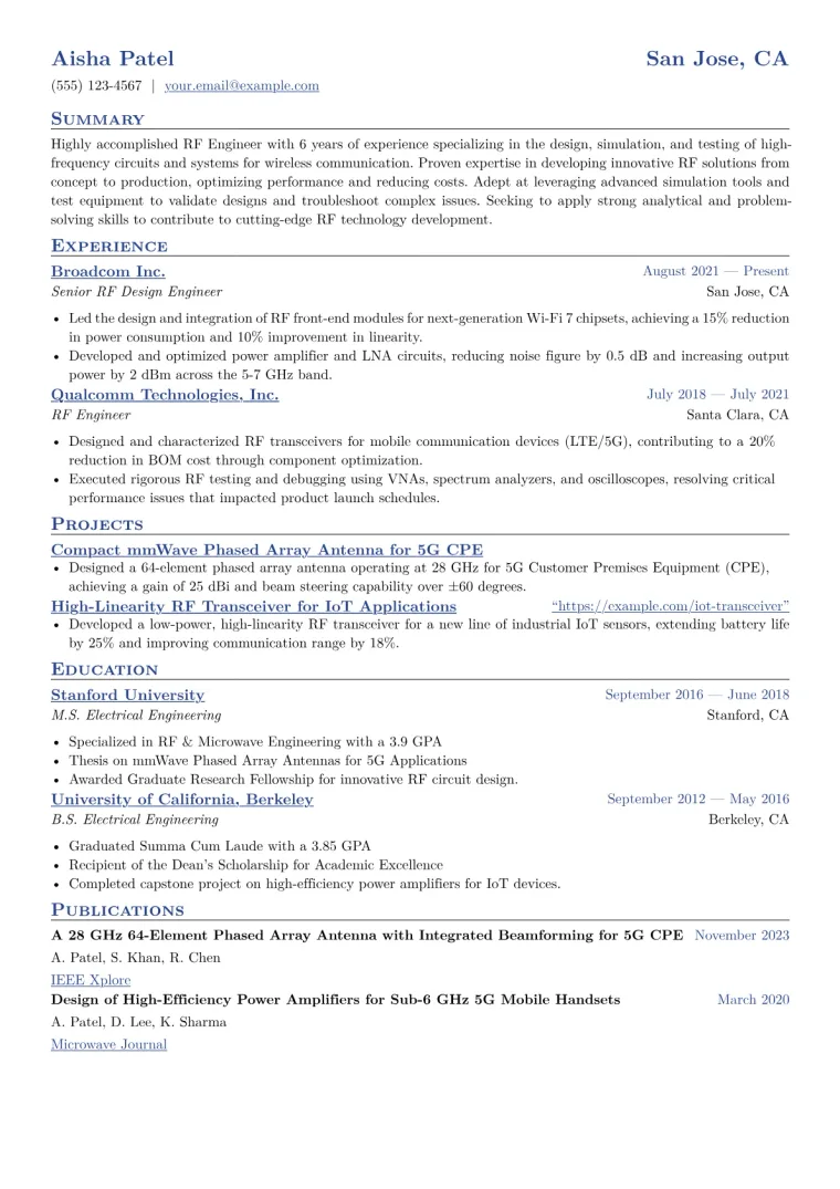
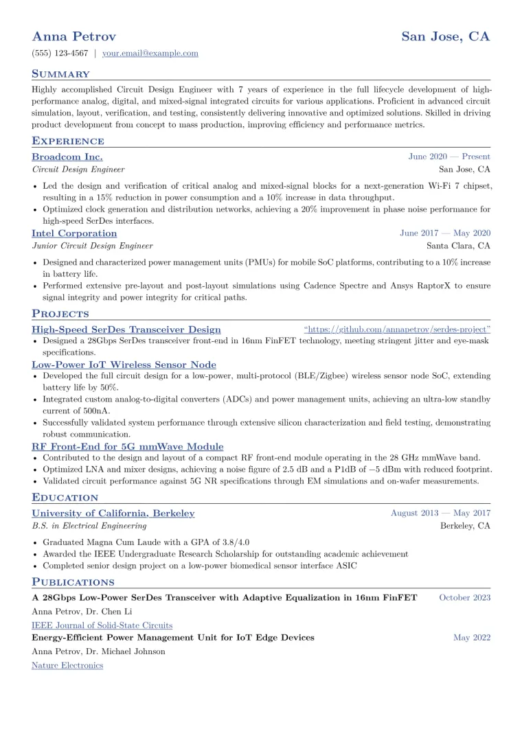
Three complete resumes, each in a different design.
Editorial Notes
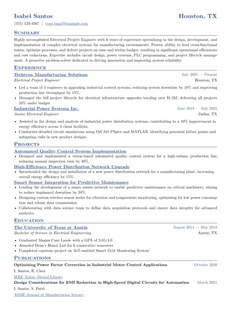
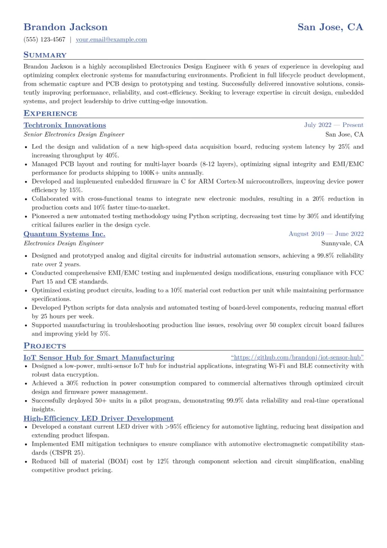
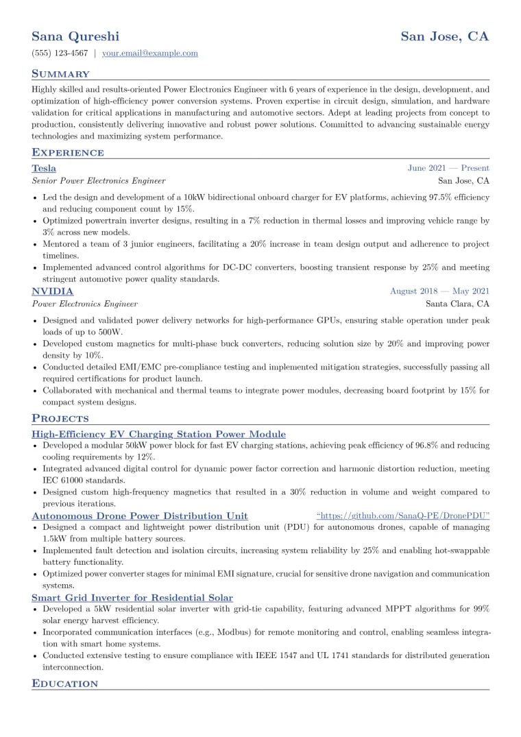
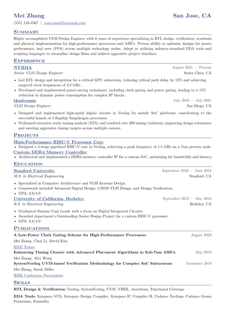
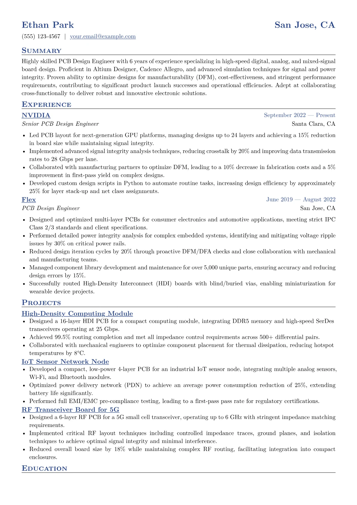
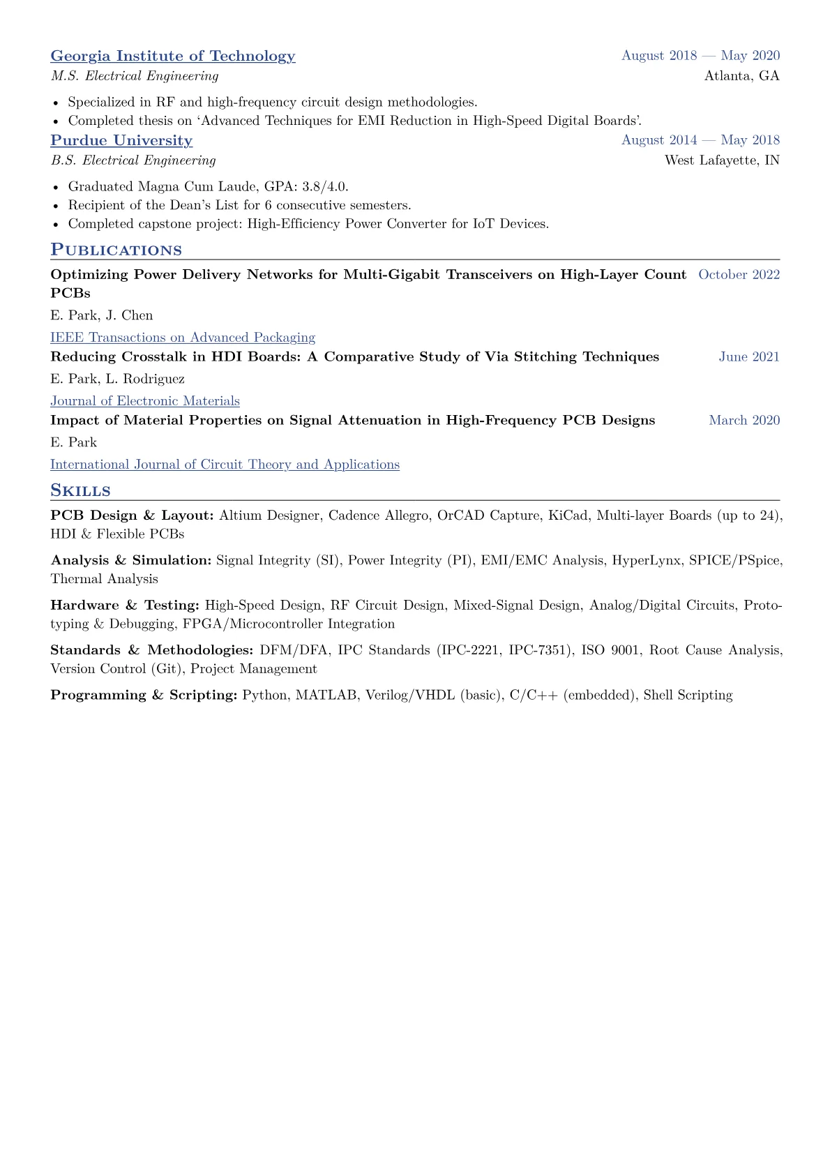
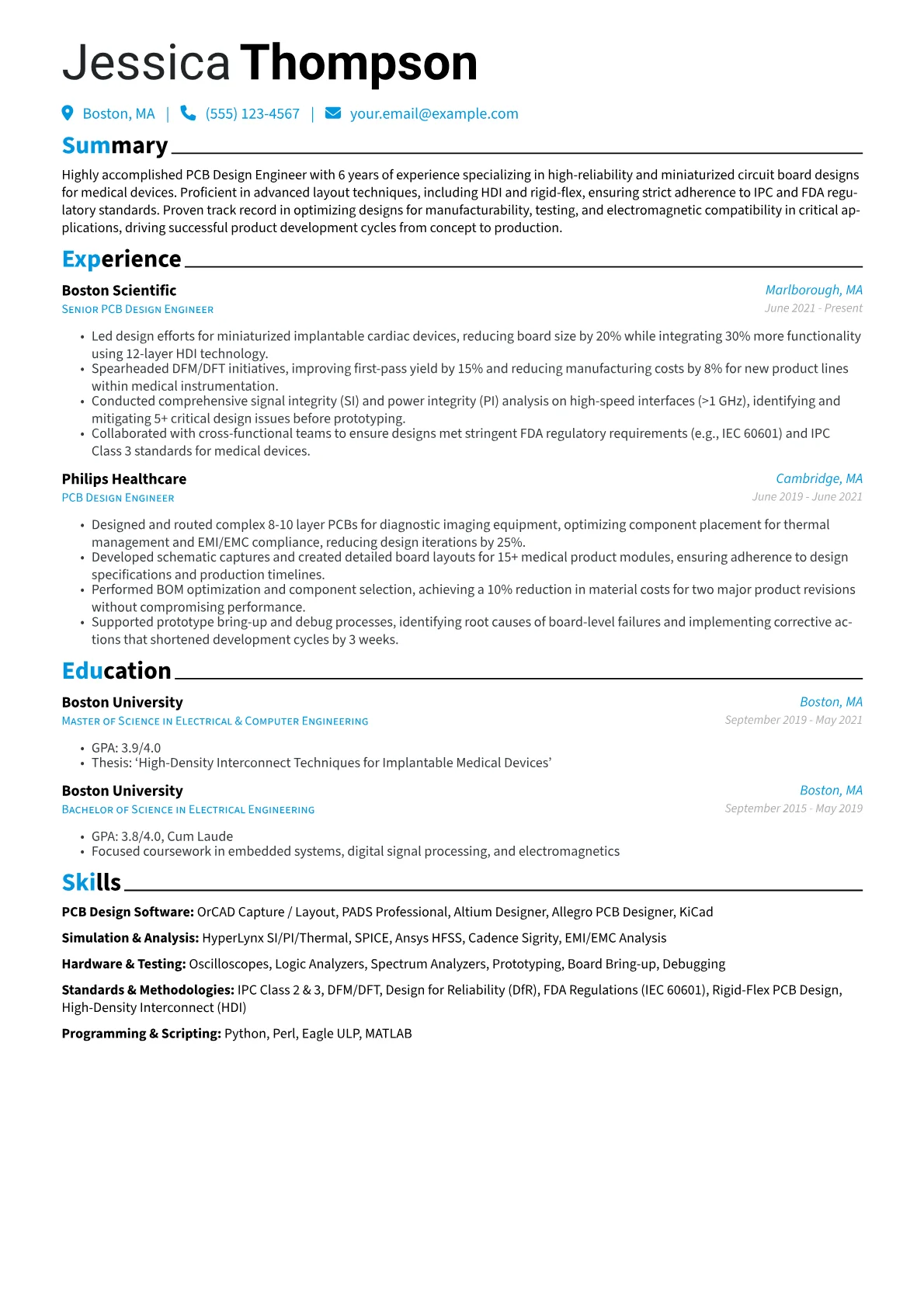
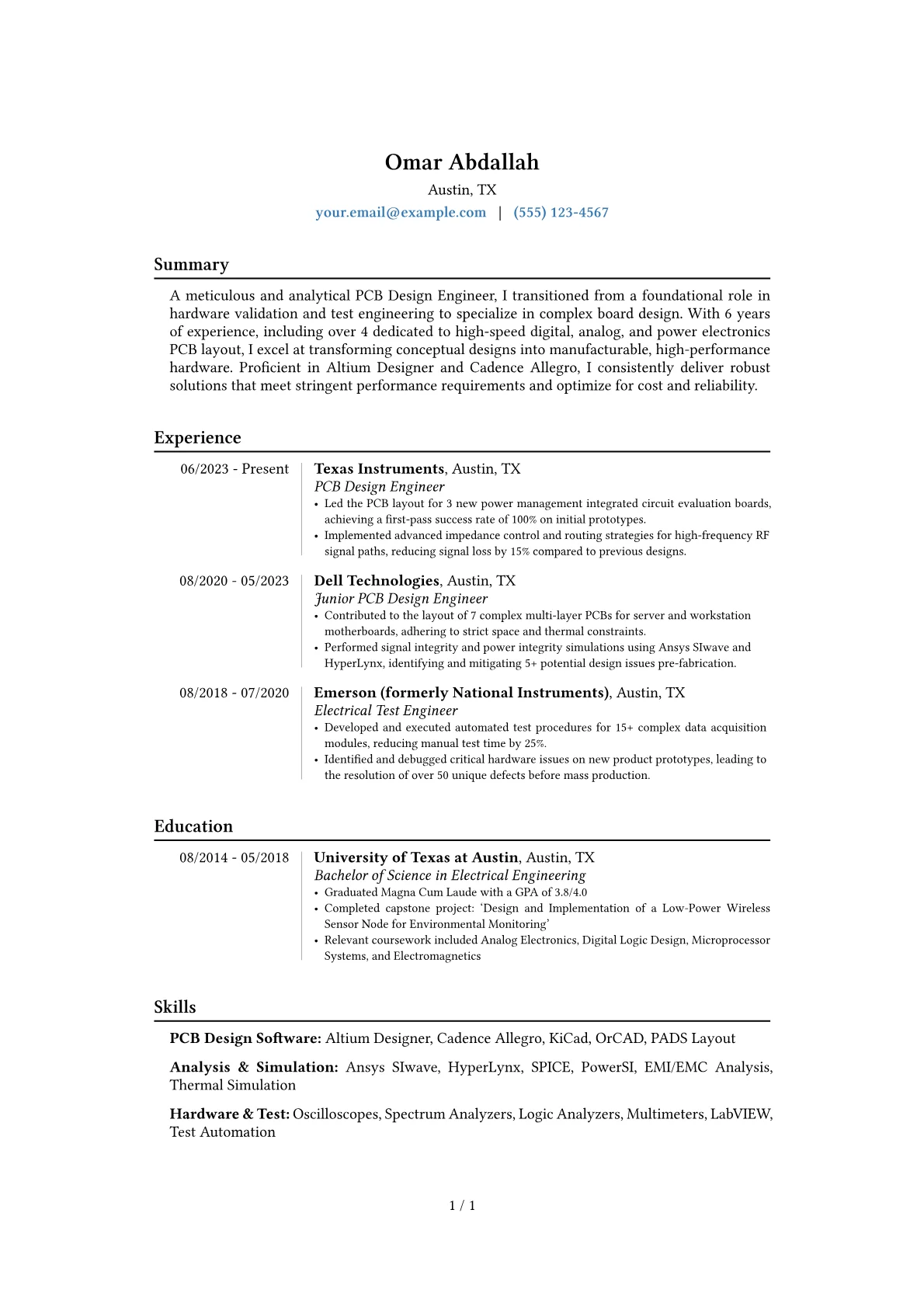
Hiring managers for PCB Design Engineer roles in Manufacturing seek candidates who demonstrate deep technical proficiency and an understanding of production realities. A strong resume highlights expertise in ECAD tools like Altium Designer or OrCAD, coupled with adherence to IPC standards such as IPC-2221 and IPC-7351. Concrete achievements should involve DFM (Design For Manufacturability), signal integrity (SI) analysis for high-speed designs, and EMI/EMC mitigation. Mentioning cost reductions, yield improvements, or board size optimizations for specific product lines significantly impresses, as does experience with multi-layer designs and thermal management.
The JobSprout PCB Design Engineer resume example effectively showcases these critical elements. It quantifies achievements like "reduced component count by 15% across three product redesigns" or "implemented DFM principles, improving first-pass manufacturing yield by 8%." Key ECAD tools and certifications (e.g., CID+) are prominently highlighted, making the candidate's technical stack immediately clear. Skills are thoughtfully grouped into categories such as "Circuit Design," "Layout & Routing," and "Compliance & Testing," providing an organized and comprehensive overview for recruiters.
This template was built with JobSprout and can be remixed to create your own tailored PCB Design Engineer resume, ready to impress manufacturing hiring teams.
How useful was this template?
Example by JobSproutPCB Design Engineer resume summary example
Highly skilled PCB Design Engineer with 6 years of experience specializing in high-speed digital, analog, and mixed-signal board design. Proficient in Altium Designer, Cadence Allegro, and advanced simulation techniques for signal and power integrity. Proven ability to optimize designs for manufacturability (DFM), cost-effectiveness, and stringent performance requirements, contributing to significant product launch successes and operational efficiencies. Adept at collaborating cross-functionally to deliver robust and innovative electronic solutions.
PCB Design Engineer salary by country
| Country | 25th percentile | Median | 75th percentile |
|---|---|---|---|
| US | $113,571 | $142,593 | $151,296 |
| UK | £38,333 | £50,000 | £58,333 |
| Canada | C$86,152 | C$113,871 | C$140,800 |
| Australia | A$101,935 | A$126,667 | A$147,857 |
| Germany | €59,500 | €70,570 | €77,887 |
| France | €37,875 | €44,167 | €49,750 |
| Netherlands | €55,000 | €66,667 | €74,250 |
| Italy | €25,000 | €31,250 | €38,750 |
| Austria | €46,250 | €58,750 | €67,500 |
| New Zealand | NZ$102,500 | NZ$120,000 | NZ$162,500 |
| India | ₹455,000 | ₹910,000 | ₹1,365,000 |
| Poland | zł186,440 | zł209,338 | zł232,236 |
Annual salaries in local currency, aggregated from live job postings via Adzuna. Figures refresh continuously and reflect advertised pay, not negotiated offers.
PCB Design Engineer resume skills and keywords
Recruiters and applicant tracking systems scan PCB Design Engineer resumes for these skills and keywords. Include the ones that match your experience and mirror the wording in the job description. Check your resume against them with the free ATS checker.
Hard skills
Tools & software
Certifications
Soft skills
Market Insights
PCB Design Engineer
Salary Range
US market data · Source: Adzuna · Updated Mar 2026
![How to Write a CV for Manufacturing Applications [2026 Guide]](/thumbnails/cv-for-manufacturing-applications.webp)