

Summary
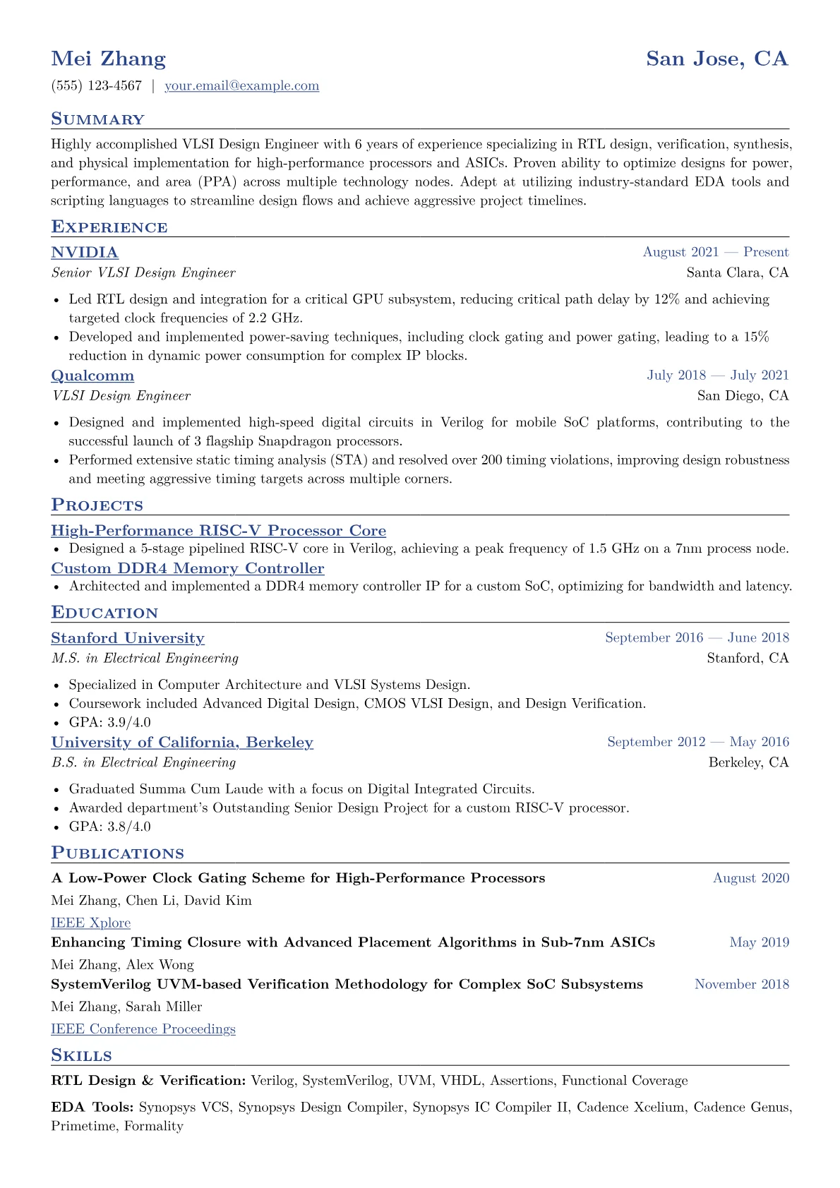
Highly accomplished VLSI Design Engineer with 6 years of experience specializing in RTL design, verification, synthesis, and physical implementation for high-performance processors and ASICs. Proven ability to optimize designs for power, performance, and area (PPA) across multiple technology nodes. Adept at utilizing industry-standard EDA tools and scripting languages to streamline design flows and achieve aggressive project timelines.
Experience
Senior VLSI Design EngineerNVIDIA
- Led RTL design and integration for a critical GPU subsystem, reducing critical path delay by 12% and achieving targeted clock frequencies of 2.2 GHz.
- Developed and implemented power-saving techniques, including clock gating and power gating, leading to a 15% reduction in dynamic power consumption for complex IP blocks.
VLSI Design EngineerQualcomm
- Designed and implemented high-speed digital circuits in Verilog for mobile SoC platforms, contributing to the successful launch of 3 flagship Snapdragon processors.
- Performed extensive static timing analysis (STA) and resolved over 200 timing violations, improving design robustness and meeting aggressive timing targets across multiple corners.
Projects
High-Performance RISC-V Processor Core
- Designed a 5-stage pipelined RISC-V core in Verilog, achieving a peak frequency of 1.5 GHz on a 7nm process node.
Custom DDR4 Memory Controller
- Architected and implemented a DDR4 memory controller IP for a custom SoC, optimizing for bandwidth and latency.
Education
Stanford UniversityM.S. in Electrical Engineering
- Specialized in Computer Architecture and VLSI Systems Design.
- Coursework included Advanced Digital Design, CMOS VLSI Design, and Design Verification.
- GPA: 3.9/4.0
University of California, BerkeleyB.S. in Electrical Engineering
- Graduated Summa Cum Laude with a focus on Digital Integrated Circuits.
- Awarded department's Outstanding Senior Design Project for a custom RISC-V processor.
- GPA: 3.8/4.0
Publications
A Low-Power Clock Gating Scheme for High-Performance Processors
Enhancing Timing Closure with Advanced Placement Algorithms in Sub-7nm ASICs
SystemVerilog UVM-based Verification Methodology for Complex SoC Subsystems
Skills
RTL Design & Verification
VerilogSystemVerilogUVMVHDLAssertionsFunctional Coverage
EDA Tools
Synopsys VCSSynopsys Design CompilerSynopsys IC Compiler IICadence XceliumCadence GenusPrimetimeFormality
Physical Design
Static Timing Analysis (STA)Power AnalysisFloorplanningPlacement & RoutingClock Tree Synthesis (CTS)DRC/LVS
Scripting & Programming
PythonTCLPerlC++Shell ScriptingMakefiles
Digital Design
CMOSLow Power DesignASIC Design FlowFPGA PrototypingComputer ArchitectureSoC Design
![How to Write a CV for Manufacturing Applications [2026 Guide]](/thumbnails/cv-for-manufacturing-applications.webp)